
Bitmo Lab is testing an ultra-thin, bendable tracker built to fit inside items traditional trackers can’t
Updated
March 17, 2026 1:02 AM
Bitmo Lab's MeetSticker tracker. PHOTO: BITMO LAB
Location trackers have become everyday accessories for keys, bags and luggage. But as personal items grow slimmer and more design-focused — from minimalist wallets to passport sleeves and specialised gear — tracking them has become less straightforward. Most trackers are built as small, rigid discs that assume the presence of space, loops or compartments. That assumption has created a growing mismatch between modern product design and the technology meant to secure it.
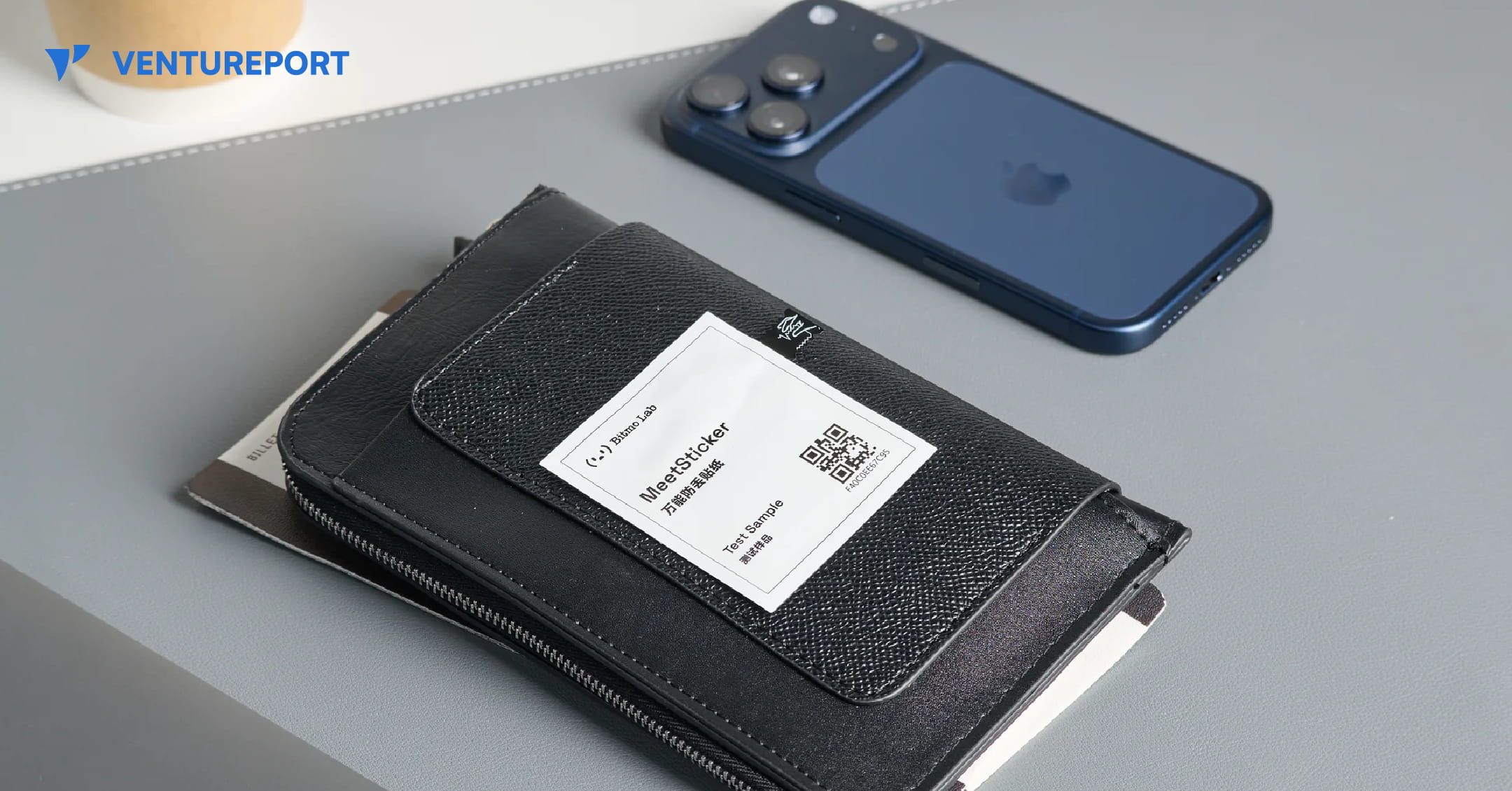
Hong Kong–based startup Bitmo Lab is attempting to address that gap with a device called MeetSticker. Instead of the solid plastic casing typical of most trackers, MeetSticker is engineered to be flexible and ultra-thin, measuring just 0.8 millimetres thick. The bendable design allows it to sit within narrow compartments or along curved surfaces without altering the shape of the object. Rather than attaching to an item externally, it is intended to integrate discreetly inside it.
That structural shift is the core of the product’s proposition. By removing the rigid shell that defines conventional tracking hardware, MeetSticker can be placed in items that previously had no practical way to accommodate a tracker. Bitmo Lab states that the device connects through a proprietary network and a companion application compatible with both iOS and Android, positioning it as a cross-platform solution rather than one tied to a single ecosystem.
The implications extend beyond form factor. Objects without obvious attachment points — such as compact travel accessories or specialised tools — could potentially be monitored without visible add-ons. In doing so, the device broadens the scope of tracking technology into categories where aesthetics, aerodynamics or compact design matter as much as functionality.
Before moving toward retail distribution, however, the company is focusing on validation. Bitmo Lab has launched a five-week global alpha testing programme beginning February 9. Sixty participants will receive a prototype unit and early access to the app. According to the company, the programme is designed to assess durability, usability and real-world performance before a wider commercial release. Participants who provide feedback will receive a retail unit upon launch.
Such testing is particularly relevant for flexible electronics. Unlike rigid devices, bendable hardware must withstand repeated flexing, daily handling and environmental exposure. Early user data can help refine manufacturing processes and software optimisation before scaling production.
As with other connected tracking devices, privacy considerations remain part of the equation. Bitmo Lab has stated that data collected during the alpha programme will be used strictly for testing purposes and deleted once the programme concludes.
Whether flexible trackers will redefine the category will depend on how they perform outside controlled testing environments. Still, the introduction of a near-invisible, bendable tracking device reflects a broader shift in consumer technology. As everyday products become thinner and more design-conscious, the tools built to protect them may need to adapt just as seamlessly.
Keep Reading
AI growth is increasingly becoming a manufacturing, packaging and deployment challenge — not just a computing one.
Updated
May 26, 2026 5:28 PM

Taipei 101 and Taipei Nan Shan Plaza, viewed from Elephant Mountain. PHOTO: UNSPLASH
As AI companies continue scaling larger models and data centers, the pressure is no longer falling only on chip design. Manufacturing capacity, advanced packaging and infrastructure deployment are becoming equally important parts of the AI race. AMD’s latest investment announcement reflects how quickly that shift is accelerating.
The US chipmaker announced plans to invest more than US$10 billion across Taiwan’s semiconductor and manufacturing ecosystem to support next-generation AI infrastructure. The investment focuses on expanding partnerships and increasing advanced packaging capacity needed for future AI systems.
The announcement highlights a growing reality across the AI industry. Building powerful AI chips is no longer enough on its own. Companies now also need the manufacturing networks, packaging technologies and supply chain coordination required to deploy AI infrastructure at global scale.
AMD’s investments center heavily around advanced chip packaging, an area becoming increasingly critical as AI systems demand higher performance and greater power efficiency. Traditional chip architectures are struggling to keep pace with the size and complexity of modern AI workloads. Advanced packaging helps connect processors, memory and computing systems more efficiently while managing power and cooling limitations inside large-scale AI environments.
The company said it is working with Taiwan-based partners including ASE, SPIL and PTI to develop next-generation packaging technologies for its upcoming 6th Gen AMD EPYC processors, codenamed “Venice.” AMD also said it had qualified what it described as the industry’s first 2.5D panel-based EFB interconnect technology alongside PTI.
At the center of the broader strategy is AMD Helios, the company’s rack-scale AI infrastructure platform scheduled for deployment beginning in the second half of 2026. The platform combines AMD Instinct MI450X GPUs, 6th Gen EPYC CPUs, networking systems and AMD’s ROCm software stack into integrated AI infrastructure systems designed for hyperscale deployment.
Rather than selling individual processors alone, companies are increasingly building complete AI infrastructure platforms that combine hardware, software, cooling systems and power management into unified deployments. That transition is reshaping how AI infrastructure is designed, manufactured and delivered.
Taiwan is also becoming more deeply embedded in that process. AMD’s investment spans not only semiconductor packaging companies but also manufacturing and system integration partners including Sanmina, Wiwynn, Wistron and Inventec. The partnerships reflect Taiwan’s growing role as one of the operational centers of the global AI infrastructure economy.
Dr. Lisa Su, Chair and CEO of AMD, said: “As AI adoption accelerates, our global customers are rapidly scaling AI infrastructure to meet growing compute demand. By combining AMD leadership in high-performance computing with the Taiwan ecosystem and our strategic global partners, we are enabling integrated, rack-scale AI infrastructure that helps customers accelerate deployment of next-generation AI systems”.
Power efficiency is becoming another major challenge shaping AI infrastructure decisions. As AI workloads consume more electricity and generate more heat, infrastructure providers are increasingly being forced to rethink cooling systems, interconnect technologies and deployment economics.
AMD’s announcement signals how the AI competition is evolving beyond model development and raw computing power. The next stage may depend just as heavily on who can manufacture, package and deploy AI infrastructure fast enough to support global demand.