
How a Korean biotech startup is using AI to move drug discovery from trial-and-error to precision design
A close up of a protein structure model. PHOTO: UNSPLASH
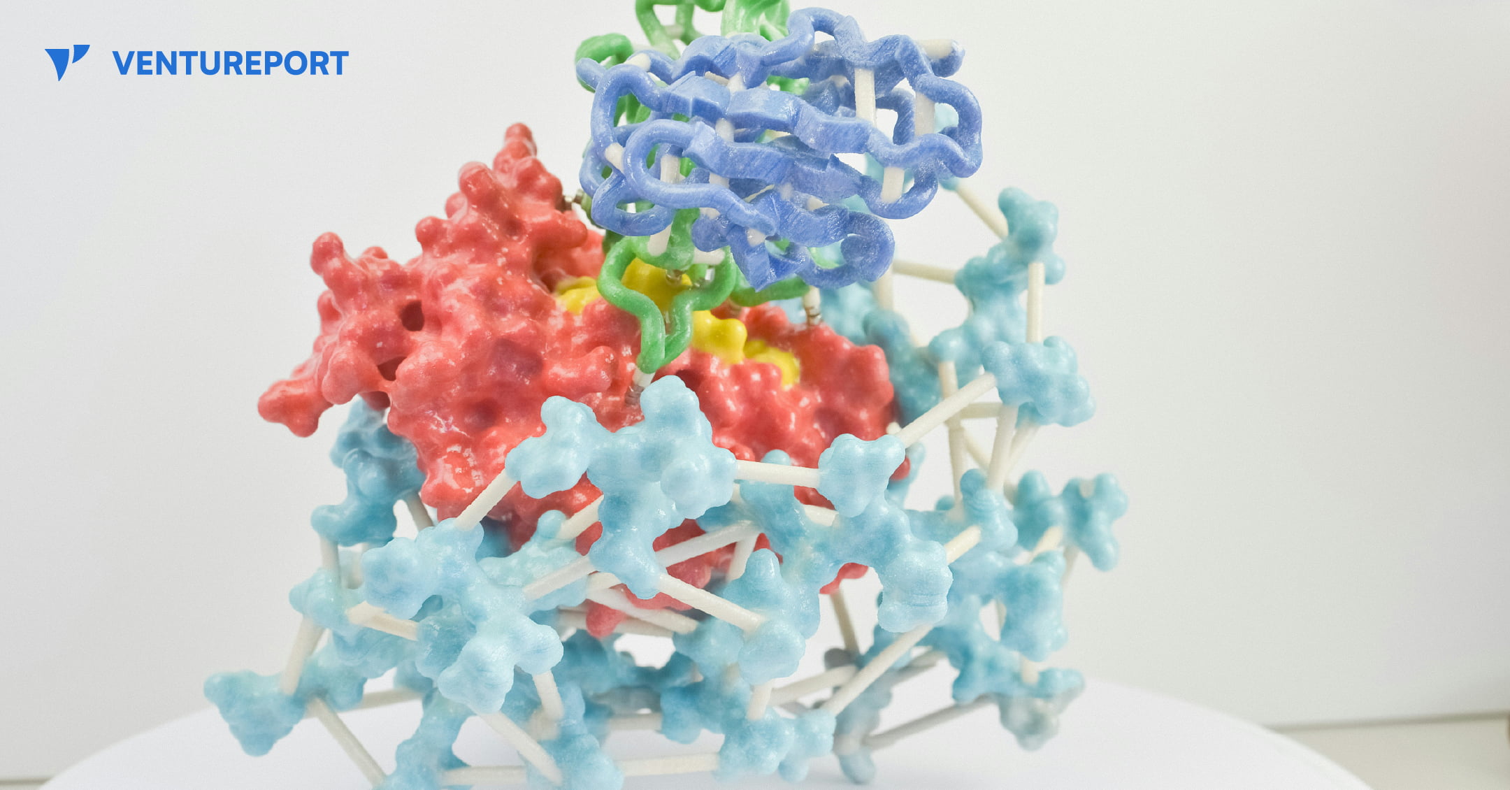
For decades, drug discovery has relied on trial and error, with scientists testing thousands of molecules to find one that works. Galux, a South Korean biotech startup, is changing that by using AI to design proteins from scratch. This method, called “de novo” design, makes it possible to build precise new therapies instead of searching through existing ones.
The company recently announced a US$29 million Series B funding round, bringing its total capital to US$47 million.This significant investment attracted a substantial roster of institutional backers, including the Korea Development Bank (KDB), Yuanta Investment, SL Investment and NCORE Ventures. These firms joined existing investors such as InterVest, DAYLI Partners and PATHWAY Investment, as well as new participants including SneakPeek Investments, Korea Investment & Securities and Mirae Asset Securities.
At the core of the company’s work is a platform called GaluxDesign. Unlike many AI tools that only predict how existing proteins fold, this system uses deep learning and physics to create entirely new therapeutic antibodies. This “from scratch” approach lets the team go after so-called “undruggable” proteins. These are targets that traditional small-molecule drugs can’t reach because they lack clear binding pockets. By designing proteins to fit these complex shapes, Galux aims to unlock treatments that have stayed out of reach for decades. And that’s exactly why investors are paying attention.
The pharmaceutical industry is actively looking for faster and more efficient ways to develop new drugs, and Galux is built for exactly that. The company connects its AI platform directly to its own wet lab, where designs can be tested in real time. Each result feeds straight back into the system, sharpening the next round of models. This continuous loop speeds up discovery and improves precision at every step. It’s also why partners like Celltrion, LG Chem and Boehringer Ingelheim are already working with Galux.
Galux is no longer just trying to make drugs that stick to a target. The company now wants its AI to design medicines that actually work in the body and can be made at scale. In simple terms, a drug has to do more than bind to a disease—it must be stable, safe and strong enough to change how the illness behaves. Galux is moving into tougher targets such as ion channels and GPCRs. These play key roles in heart function and sensory signals. Ultimately, the goal is to show that AI-driven design can turn complex biology into real treatments. And instead of hunting blindly for a solution, the team is building exactly what they need.
Keep Reading
AI growth is increasingly becoming a manufacturing, packaging and deployment challenge — not just a computing one.
Updated
May 26, 2026 5:28 PM

Taipei 101 and Taipei Nan Shan Plaza, viewed from Elephant Mountain. PHOTO: UNSPLASH
As AI companies continue scaling larger models and data centers, the pressure is no longer falling only on chip design. Manufacturing capacity, advanced packaging and infrastructure deployment are becoming equally important parts of the AI race. AMD’s latest investment announcement reflects how quickly that shift is accelerating.
The US chipmaker announced plans to invest more than US$10 billion across Taiwan’s semiconductor and manufacturing ecosystem to support next-generation AI infrastructure. The investment focuses on expanding partnerships and increasing advanced packaging capacity needed for future AI systems.
The announcement highlights a growing reality across the AI industry. Building powerful AI chips is no longer enough on its own. Companies now also need the manufacturing networks, packaging technologies and supply chain coordination required to deploy AI infrastructure at global scale.
AMD’s investments center heavily around advanced chip packaging, an area becoming increasingly critical as AI systems demand higher performance and greater power efficiency. Traditional chip architectures are struggling to keep pace with the size and complexity of modern AI workloads. Advanced packaging helps connect processors, memory and computing systems more efficiently while managing power and cooling limitations inside large-scale AI environments.
The company said it is working with Taiwan-based partners including ASE, SPIL and PTI to develop next-generation packaging technologies for its upcoming 6th Gen AMD EPYC processors, codenamed “Venice.” AMD also said it had qualified what it described as the industry’s first 2.5D panel-based EFB interconnect technology alongside PTI.
At the center of the broader strategy is AMD Helios, the company’s rack-scale AI infrastructure platform scheduled for deployment beginning in the second half of 2026. The platform combines AMD Instinct MI450X GPUs, 6th Gen EPYC CPUs, networking systems and AMD’s ROCm software stack into integrated AI infrastructure systems designed for hyperscale deployment.
Rather than selling individual processors alone, companies are increasingly building complete AI infrastructure platforms that combine hardware, software, cooling systems and power management into unified deployments. That transition is reshaping how AI infrastructure is designed, manufactured and delivered.
Taiwan is also becoming more deeply embedded in that process. AMD’s investment spans not only semiconductor packaging companies but also manufacturing and system integration partners including Sanmina, Wiwynn, Wistron and Inventec. The partnerships reflect Taiwan’s growing role as one of the operational centers of the global AI infrastructure economy.
Dr. Lisa Su, Chair and CEO of AMD, said: “As AI adoption accelerates, our global customers are rapidly scaling AI infrastructure to meet growing compute demand. By combining AMD leadership in high-performance computing with the Taiwan ecosystem and our strategic global partners, we are enabling integrated, rack-scale AI infrastructure that helps customers accelerate deployment of next-generation AI systems”.
Power efficiency is becoming another major challenge shaping AI infrastructure decisions. As AI workloads consume more electricity and generate more heat, infrastructure providers are increasingly being forced to rethink cooling systems, interconnect technologies and deployment economics.
AMD’s announcement signals how the AI competition is evolving beyond model development and raw computing power. The next stage may depend just as heavily on who can manufacture, package and deploy AI infrastructure fast enough to support global demand.